Speaker: Dr. John H Lau, ASM Pacific Technology

Presentation Slides: “Fan-Out Wafer-Level Packaging
for 3D IC Heterogeneous Integration” (3.4 MB PDF)
Meeting Date: Thursday, January 25, 2018
Time: 11:30 AM Registration (and sandwiches/drinks); 12:00 PM Presentation
Presentation-only (no cost): 12:00 noon (come at 11:45)
Cost: $5 IEEE members. students, unemployed, $10 non-members
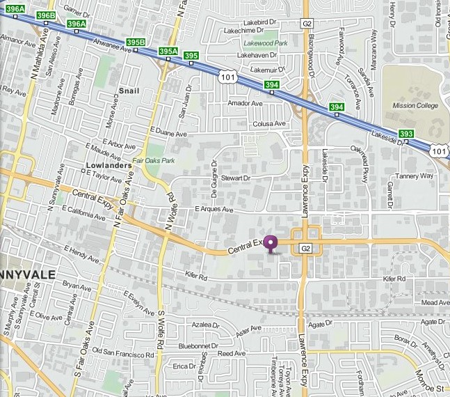
Location: Texas Instruments Building E Conference Center, 2900 Semiconductor Dr. (off Kifer Rd), Santa Clara
Reservations: 1801eps.eventbrite.com
Summary: Because of the drive of Moore’s law, compounded with the demands of mobile products such as smartphones and tablets, SoC (system-on-chip) has been very popular in the past 10+ years. SoC integrates ICs with different functions into a single chip for the system or subsystem. Unfortunately, the end of Moore’s law is fast approaching and it is more and more difficult and costly to reduce the feature size (to do the scaling) to make the SoC. Heterogeneous integration contrasts with SoC. It has been a very “fancy” name in semiconductor packaging for the past few years. Heterogeneous integration uses packaging technology to integrate dissimilar chips with different functions into a system or subsystem, rather than integrating all the functions into a single chip and go for finer feature size. For the next five years, we will see more implementations of a higher level of heterogeneous integration, whether it is for performance, form factor, power consumption or cost. SiP (system-in-package) is similar to heterogeneous integration but with less density and lower gross pitch. In this lecture, the following topics will be presented. Emphasis is placed on the latest developments of these areas in the past three years. Their future trends will also be explored.
SoC: Apple’s application processor (A10 and A11)
SiP: Amkor’s SiP for automobiles; Apple Watch II (S2) assembled by ASE
Heterogeneous Integration with SoW (System-on-Wafer): Leti’s SoW; ULCA’s SoW
Heterogeneous Integration with TSV-Interposers: TSMC/Xilinx’s CoWoS; AMD’s GPU with Hynix’s HBM and UMC’s TSV-interposer; Nvidia’s GPU with Samsung’s HMB2 and TSMC’s TSV-interposer
Heterogeneous Integration with TSV-less Interposer: Xilinx/SPIL’s TSV-less SLIT; SPIL/Xilinx’s TSV-less NTI; Amkor’s TSV-less SLIM; ASE’s TSV-less FOCoS; MediaTek’s TSV-less RDLs by FOWLP; Intel’s TSV-less EMIB; Intel/AMD’s TSV-less EMIB for CPU, GPU, and HBM; Intel’s Knight-Landing with Micron’s HMC on TSV-less Organic Interposer; Cisco/eSilicon’s TSV-less Organic Interposer; ITRI’s TSV-less TSH; Shinko’s TSV-less i-THOP

Bio: John H. Lau has been a senior technical advisor of ASM since 2014, an ITRI Fellow of Industrial Technology Research Institute for 4.5 years, a visiting professor at HKUST for 1 year, the Director of MMC Laboratory with IME Singapore for 2 years and a Senior Scientist/MTS at HPLab/Agilent in California for more than 25 years. With more than 39 years of R&D and manufacturing experience in semiconductor packaging, he has published more than 450 peer-reviewed papers, 30 issued and pending patents, and 18 textbooks on flip chip technologies, WLCSP, BGA, TSV for 3D integration, advanced MEMS packaging, and reliability of 2D and 3D IC interconnections. John received many awards and is an elected ASME Fellow and has been an IEEE Fellow since 1994.