
Date: Thursday, February 22, 2018
Time: 8:30 AM to 6:00 PM
Cost: $40 IEEE members. students, unemployed, $50 non-members ($10 more, after Feb. 9th)
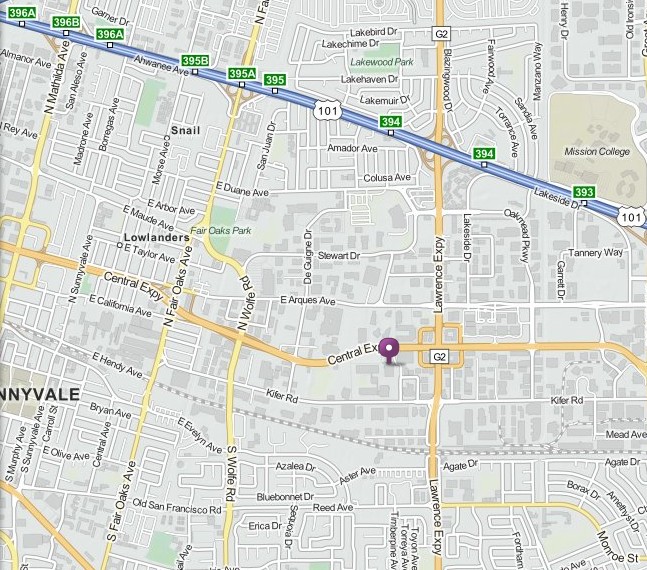
Location: Texas Instruments Building E Conference Center, 2900 Semiconductor Dr. (off Kifer Rd), Santa Clara
Reservations: 1802symp-eps.eventbrite.com
Program Outline:
— Download Full Program, Hotel Recommendations
— Presentations from HIR Technical Working Group chairs
— Overview from HIR International Roadmap Committee
Sponsors:


We thank our financial supporters:


Summary: We are entering the era of the digital economy and myriad connectivity with data migration to the cloud, smart devices everywhere, the Internet of Everything, and the emergence of autonomous vehicles. Artificial Intelligence and big data analytics are undergirding all market segments.
As we approach the inflection point of explosive expansion of innovations and electronic products into global society, and the plateauing of CMOS’s scaling advantage, continued progress will require a different phase of electronics innovation. Heterogeneous Integration is and will be the key technology direction going forward. It is the “low hanging fruit” for initiating a new era of technological and scientific advances to continue and complement the progression of Moore’s Law scaling into the distant future.
A Heterogeneous Integration Roadmap is critically needed to focus on new materials and new devices, new architecture, designs, manufacturing processes and new methodologies to bring diverse components together into a System-in-Package (SiP). It will be a pre-competitive technology roadmap addressing future vision, difficult challenges, and potential solutions serving the industry, academia, government labs and research institutes and in fact our own profession.

We firmly believe that the Heterogeneous Integration Roadmap, founded with initiative from the three IEEE Societies — EPS, EDS & Photonics — and in collaboration with SEMI & ASME’s EPPD, has expanded to embrace innovations wherever they arise and promote collaboration wherever possible to accelerate progress in this disruptive digital landscape. Heterogeneous Integration requires a diverse set of disciplines and addresses a broad spectrum of applications. We have developed a broad and inclusive worldview to comprehend this diversity and assembled a group of leading technical experts to develop the Roadmap. The first work product of the Roadmap team will be presented by the chairs of the 20 Technical Working Groups for review and feedback.
 Plenary Talk: “Synergistic Growth of AI and Silicon Age 4.0 through Heterogeneous Integration of Technologies” — Dr. Nicky Lu, Chairman, CEO & Founder, Etron Technology, Inc., and Managing Board Director, Taiwan Semiconductor Industry Association (TSIA)
 Closing Remarks — Dr. Gaurang N. Choksi, Intel: Vice President, Technology and Manufacturing Group; Director, Assembly and Test Technology Development Core Competencies
Program Agenda
8:30: Registration and refreshments
9:00: Start of Program
Download Full Program, with topics, speakers
5:30 – 6:00 pm Wrap-Up
Roadmap Working Groups:
HI for Market Applications
• Mobile
• IoT
• Medical and Health & Wearables
• Automotive
• High Performance Computing and Data Center
• Aerospace and Defense
Heterogeneous Integration Components
• Single-Chip and Multi-Chip Packaging (including Substrates)
• Integrated Photonics
• Integrated Power Electronics
• MEMS & Sensor Integration
• RF and Analog Mixed-Signal Design
• Co-Design and Simulation – Tools & Practice
Cross Cutting topics
• Materials & Emerging Research Materials
• Emerging Research Devices
• Interconnect
• Test
• Supply Chain
• Security (Cyber)
Integration Processes
• SiP
• 3D +2.5D
• WLP (fan in and fan out)
 Bio: As a researcher, design architect, entrepreneur and chief executive, Dr. Nicky Lu has dedicated his career to the worldwide IC design and semiconductor industry. He also co-founded several other high-tech companies including Ardentec, Global Unichip and GTBF Corporations. Dr. Lu worked for the IBM Research Division and then the Headquarters from 1982 to 1990 and won numerous IBM recognition awards, including an IBM Corporate Award. He co-invented and pioneered a 3D-DRAM technology, known as the Substrate-Plate Trench-Capacitor (SPT) cell, along with its associated array architecture, which has been widely used by IBM and its licensees from 4Mb to 1Gb DRAMs and embedded DRAMs over hundreds of billions dollars. Dr. Lu designed several High-Speed CMOS DRAM (HSDRAM) chips, with all top worlds’ records of performance. He was a co-architect leading the 8-inch wafer and DRAM/SRAM/LOGIC technology developments for Taiwan semiconductor industry in early 1990s, also created many Taiwan companies as prominent silicon-chip suppliers. Since 1999 he has pioneered Known-Good-Die Memory Products enabling 3D stacked-dices system chips; this work summoned the new rise of an IC Heterogeneous Integration Era as described in his ISSCC-2004 plenary talk, demonstrating a new 3D-IC trend. He was a keynote speaker at the 2016 A-SSCC disclosing Silicon-Age-4.0 Era with a new Virtual Moore’s Law as a indicator of continual economic growth.
Dr. Lu received his B.S. in Electrical Engineering from National Taiwan University and M.S. and Ph.D. in EE from Stanford University. He holds over 30 U.S. patents and has published more than 60 technical papers. He serves as Managing Board Director and was Chairman of TSIA, as Board Member of Global Semiconductor Alliance (GSA) and GSA’s General Chair (2009 to 2011), and Chairman of WSC (World Semiconductor Council) from 2014 to 2015. He received the Scientific Management Award (2012) from Chinese Society for Management of Technology and Taiwan’s Golden Merchant Award (2007) from General Chamber of Commerce. He is an Outstanding Alumnus of National Taiwan University, a Chair Professor and an Outstanding Alumnus of National Chiao Tung University, an IEEE Fellow, the recipient of the IEEE 1998 Solid-States Circuits Award, a member of NAE (National Academy of Engineering of USA), and recipient of a SEMI Industry Contribution Award in 2017.

Bio: William (Bill) Chen currently holds the position of ASE Fellow and Senior Technical Advisor at ASE Group. Prior to joining ASE, he was the Director at the Institute of Materials Research & Engineering in Singapore. Bill retired from IBM Corporation after a career spanning over thirty years in various R&D and managerial positions. He has held adjunct and visiting faculty positions at Cornell University, Hong Kong University of Science and Technology, and Binghamton University. Bill is the chair of the newly formed Heterogeneous Integration Technology Roadmap for Semiconductors, an initiative addressing technologies for the IoT/IoE/cloud computing era, jointly sponsored by IEEE EPS, EDS, Photonics Societies, ASME’s EPPD, and SEMI. He also chairs SEMI’s Advanced Packaging Committee. In 2009, Bill received the InterPACK Excellence Award for his contributions, and in 2010, he was presented with the IEEE EPS Society David Feldman Outstanding Contribution Award. He is a past President of the IEEE EPS Society and he has been elected a Fellow of IEEE and a Fellow of ASME. Bill received his B. Sc. from London University, M.Sc. from Brown University and Ph.D. from Cornell University.

Bio: Dr. W. R. “Bill” Bottoms, the holder of a Ph.D. from Tulane University, has an extensive background in academia, venture funding, and in the commercial semiconductor equipment sector. Since founding 3MTS in 1999, Bill Bottoms has provided strategic leadership and vision in keeping with the promise of the 3MTS business model. Dr. Bottoms has also served on a number of important government and industry committees and advisory positions. Key posts include chairmanship of the subcommittee of the Technical Advisory Committee of the United States Commerce Department’s Export Control Commission for Semiconductor Equipment and Materials.
Shortly after receiving his doctorate in physics, Dr. Bottoms joined the electrical engineering faculty of Princeton University, where he remained until 1976. He then joined Varian Associates in Palo Alto, as manager of research and development, and he was later named president of Varian’s newly formed semiconductor equipment group. After leaving Varian, he was senior vice president and general partner at Patricof & Co. Ventures, Inc., an international venture capital firm. He founded Third Millennium Test Solutions in March 1999.