
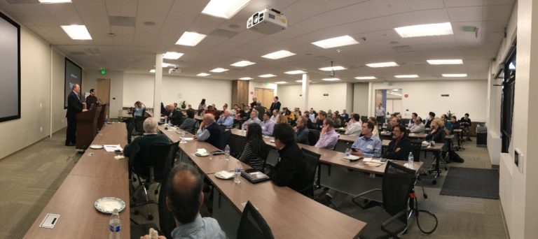
Dr. Ivor Barber of AMD presenting at one of our luncheon talks.
Visit our Program Committee Page
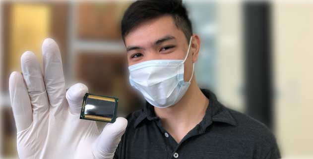
An advanced pre-production package, held by UC-Davis graduate A. Nguyen, a packaging engineer

Annette Teng
Welcome, and thank you for visiting our IEEE-EPS-Silicon Valley Chapter website. Whether you are IEEE member or casual onlooker, we hope you can enjoy our website and find us of value to you.
Since our inception over 50 years ago, EPS-SCV has provided a valuable forum for those who are interested in learning and exchanging knowledge relating to electronic packaging design, assembly, test, thermal and stress management. Our chapter is a facilitator for sharing knowledge and networking with others through activities such as lunch talks, symposiums and factory visits. We normally hold a monthly lunch seminar at SEMI Headquarters in Milpitas. However, since the shelter-in-place came into effect, we have organized a series of EPS webinars in the area of device package heterogeneous integration and the HI Roadmap. Slides and videos from past seminars can be downloaded/viewed from this webpage. Membership is not required to attend nor required to download/view past content. We are in various stages of organizing more webinars and virtual symposiums for the rest of this year.
Our last face to face seminar was on Feb 28, 2020 with a talk by John Lau, and our last symposium was Feb 20, 2020 — the Third Annual Heterogeneous Integration Roadmap (HIR) Symposium, with 170 attendees. Thankfully, no one was infected from attending either event.
Our membership is made up of a few hundred Bay Area members who are currently employed or have previously worked in high tech firms (and academia) in the area of device packaging. Those of us keeping the chapter active consist of a committee of officers who are voted in yearly. If interested, you can become an IEEE-EPS member by going to the EPS Website; also, we have many opportunities within the chapter for you to get involved — such as outreach programs to promote packaging interests to students and also to provide funding to underserved groups.
Home | Contact IEEE Santa Clara Valley Chapter, EPS | Accessibility | Privacy & Opting Out of Cookies | Nondiscrimination Policy
IEEE Santa Clara Valley Chapter, EPS, Serving Silicon Valley and the SF Bay Area. © Copyright 2022 IEEE – All rights reserved. Use of this Web site signifies your agreement to the IEEE Terms and Conditions
.A not-for-profit organization, IEEE is the world’s largest technical professional organization dedicated to advancing technology for the benefit of humanity.2
Home | Contact IEEE Santa Clara Vally Chapter, EPS | Accessibility | Privacy & Opting Out of Cookies | Nondiscrimination Policy
IEEE Santa Clara Valley Chapter, EPS
Serving Silicon Valley and the SF Bay Area
© Copyright 2020 IEEE – All rights reserved. Use of this Web site signifies your agreement to the IEEE Terms and Conditions.
A not-for-profit organization, IEEE is the world’s largest technical professional organization dedicated to advancing technology for the benefit of humanity.