 Dr. Debendra Das Sharma is an Intel Senior Fellow and co-GM of Memory and I/O Technologies in the Data Platforms and Artificial Intelligence Group at Intel Corporation. He is a leading expert on I/O subsystem and interface architecture. Das Sharma is a member of the Board of Directors for the PCI Special Interest Group (PCI-SIG) and a lead contributor to PCIe specifications since its inception. He is a co-inventor and founding member of the CXL consortium and co-leads the CXL Technical Task Force. He co-invented the chiplet interconnect standard UCIe and is the chair of the UCIe consortium. Das Sharma has a bachelor’s in technology (with honors) degree in Computer Science and Engineering from the Indian Institute of Technology, Kharagpur and a Ph.D. in Computer Engineering from the University of Massachusetts, Amherst. He holds 160+ US patents and 400+ patents world-wide. He is a frequent keynote speaker, plenary speaker, distinguished lecturer, invited speaker, and panelist at the IEEE Hot Interconnects, IEEE Cool Chips, IEEE 3DIC, SNIA SDC, PCI-SIG Developers Conference, CXL consortium, Open Server Summit, Open Fabrics Alliance, Flash Memory Summit, Intel Innovation, various Universities (CMU, Texas A&M, UIUC), and Intel Developer Forum. He has been awarded the Distinguished Alumnus Award from Indian Institute of Technology, Kharagpur in 2019, the IEEE Region 6 Outstanding Engineer Award in 2021, the first PCI-SIG Lifetime Contribution Award in 2022, and the IEEE Circuits and Systems Industrial Pioneer Award in 2022. |
 Dr. Xin Wu is Corporate Vice President of Silicon Technology, Advanced Micro Devices, Inc. (AMD). He received his PhD and MSc from University of California Berkeley and Peking University, China, respectively. Since 1993, he has worked at Xilinx (acquired by AMD in 2022) from the 0.6um through the 2nm generations of technologies and products, from many foundries. His responsibilities include silicon, hetero-integration, advanced packaging, thermal mechanical solutions and the development of many other technologies. Dr. Xin Wu is Corporate Vice President of Silicon Technology, Advanced Micro Devices, Inc. (AMD). He received his PhD and MSc from University of California Berkeley and Peking University, China, respectively. Since 1993, he has worked at Xilinx (acquired by AMD in 2022) from the 0.6um through the 2nm generations of technologies and products, from many foundries. His responsibilities include silicon, hetero-integration, advanced packaging, thermal mechanical solutions and the development of many other technologies.
|
|
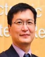 Wei-Chung Lo, Industrial Technology Research institute (ITRI) Wei-Chung Lo, Industrial Technology Research institute (ITRI)Summary: Artificial Intelligence(AI) has become the global big thing of our data-driven era, and “AI on a Chip” is considered a core competence of every smart device in the future. This presentation shares the key aspects of the “AI-on-a-Chip” Program in Taiwan as well as the achievement and Special-Interests Groups (SIGs) of AI-on-Chip Taiwan Alliance (AITA). AI-on-Chip program keeps the momentum to speed up the market-oriented research and development to fulfill the domain-specific needs of smart living, quality of life and a sustainable environment by adopting both innovative Silicon IP and advanced heterogeneous integration technology. We will share the up-to-date of results and development of AI-on-Chip technology including “AI Chip Application”, “Heterogeneous AI Chip Integration”, “Emerging AI Processing Architecture” and “AI System Software”. All these results can further leverage Taiwan’s strength in the semiconductor and ICT fields and continue to contribute to the world with its advances in AI Technologies. Wei-Chung Lo is the Deputy General Director, Electronic and Optoelectronic System Research Laboratories (EOSL), Industrial Technology Research institute (ITRI). He received his PhD from the National Taiwan University in Chemistry, and attended the Wharton school AMP+ program in 2010. He has served as Chairman of IMAPS Taiwan, the 3D IC/Panel Fan-Out consortium, the Advanced Microsystem and Packaging Alliance (AMPA), and Program Chair of IMPACT 2009/2015/2018 (IEEE-EPS). He is a member of the ECTC subcommittee on interconnects and is Co-Chair of the SEMI Packaging and Test committee. He received the SEMI Industry Contribution Award, the CIE Outstanding Engineer Award, the CPMA National Manager Excellence Award, and the ROC Innovation Elite Award. |
 Prof. Madhavan Swaminathan, is the Department Head of Electrical Engineering at Penn State University. He also serves as the Director for the Center for Heterogeneous Integration of Micro Electronic Systems (CHIMES), an SRC JUMP 2.0 Center. Prior to joining Penn State, he was the Chair in Microsystems Packaging & Electromagnetics in the School of Electrical and Computer Engineering (ECE), Professor in ECE with a joint appointment in the School of Materials Science and Engineering (MSE), and Director of the 3D Systems Packaging Research Center (PRC), Georgia Tech. Prior to GT, he was with IBM working on packaging for supercomputers. Prof. Madhavan Swaminathan, is the Department Head of Electrical Engineering at Penn State University. He also serves as the Director for the Center for Heterogeneous Integration of Micro Electronic Systems (CHIMES), an SRC JUMP 2.0 Center. Prior to joining Penn State, he was the Chair in Microsystems Packaging & Electromagnetics in the School of Electrical and Computer Engineering (ECE), Professor in ECE with a joint appointment in the School of Materials Science and Engineering (MSE), and Director of the 3D Systems Packaging Research Center (PRC), Georgia Tech. Prior to GT, he was with IBM working on packaging for supercomputers.He is the author of 550+ refereed technical publications and holds 31 patents. His publications have been recognized through 32 best paper awards. He is the primary author and co-editor of 3 books and 5 book chapters, founder and co-founder of two start-up companies, and founder of the IEEE Conference on Electrical Design of Advanced Packaging and Systems (EDAPS), a premier conference sponsored by the IEEE Electronics Packaging Society (EPS). He is a Fellow of IEEE, Fellow of the National Academy of Invetors (NAI), and has served as the Distinguished Lecturer for the IEEE Electromagnetic Compatibility (EMC) society. His major accomplishment is the graduation of 73 students (49 PhD & 24 MS) during his career (so far) who hold leadership positions in industry. He received his MS and PhD degrees in Electrical Engineering from Syracuse University in 1989 and 1991, respectively. |
|
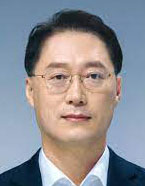 Dr. Moonsoo Kang, Executive Vice President, Head of Advanced PKG Business, Device Solutions Division of Samsung Electronics Co., Ltd. Dr. Moonsoo Kang, Executive Vice President, Head of Advanced PKG Business, Device Solutions Division of Samsung Electronics Co., Ltd.Appointed as the new head of AVP Business unit in Dec. 2022, Executive Vice President Moonsoo Kang is responsible for the entire Advanced packaging business, including development and manufacturing in Samsung Device Solutions Division. Before his new role, Dr. Kang led the Business Development Team at Samsung Foundry BU, responsible for executing marketing strategies and technology planning since 2019. Prior to joining Samsung, he had taken several key positions within Physical Integration and Designing departments, contributing to his extensive experience in the semiconductor industry since 2005. He was also a professor of Physics at Washington State University, US in 2001 – 2005. His experience and insight of the industry has greatly contributed in founding new business for Advanced Packaging in Samsung. |
 Dr. Scott Sikorski, Technology Business Development, IBM Corp. Dr. Scott Sikorski, Technology Business Development, IBM Corp.Dr. Scott Sikorski rejoined IBM in early 2020 with responsibility for growing IBM’s AI hardware partner ecosystem, and is based out the T.J. Watson Research Center. Previously, Dr. Sikorski was with STATS ChipPAC for 10 years during which he held leadership positions in Product Line Management and Business Development before being promoted to head of Corporate Strategy in late 2012. In this role he assisted in the acquisition by JCET Group in 2015 at which point he was named Vice President of Product Technology Marketing. In December 2017, Dr. Sikorski was appointed VP of Group Technology Strategy. Dr. Sikorski served on the Boards of industry organizations iNEMI and MEPTEC for several years. Dr. Sikorski started his career in 1989 with IBM Microelectronics, holding positions in R&D, Manufacturing, Product Line Management, Business Development and Complex Deal Negotiation over a 20-year period. Dr. Sikorski received his Bachelor of Science degree from Columbia University’s School of Engineering and Applied Sciences in Metallurgical Engineering and his Master’s degree and Ph.D. from the Massachusetts Institute of Technology, both in Materials Engineering. |
|
 Robert Rudnitsky, US National Institute of Standards and Technology (NIST) Office of Advanced Manufacturing Associate Director and Acting Division Chief for Policy and Strategy Robert Rudnitsky, US National Institute of Standards and Technology (NIST) Office of Advanced Manufacturing Associate Director and Acting Division Chief for Policy and StrategyRobert Rudnitsky is a Physicist and is the Associate Director at the National Institute of Standards and Technology (NIST) Office of Advanced Manufacturing, where he also serves as Acting Division Chief of Policy and Strategy. Robert received a Ph.D. in Applied Physics from Stanford University, where he was a Hertz Fellow, and a B.A. from Yale University. At Stanford, his research was at the intersection of microelectromechanical systems (MEMS), nanotechnology, and biotechnology. He designed and fabricated advanced MEMS sensors to measure the binding forces between pairs of protein molecules, and developed thermodynamic models of the molecular interactions. Prior to coming to NIST as Scientific Advisor to the Director of the Center for Nanoscale Science and Technology, Robert worked as a Physicist in the U.S. State Department in the Office of Space and Advanced Technology, where he chaired the U.S. National Nanotechnology Initiative (NNI) Global Issues in Nanotechnology Working Group, which coordinated United States Government international activities related to nanotechnology. He was also elected the founding chair of the international Organisation for Economic Cooperation and Development (OECD) Working Party on Nanotechnology. As Associate Director and Acting Division Chief, Robert provides scientific and technical guidance for the Manufacturing USA program, and develops policy and strategy for new programs, including the planning for the CHIPS Research and Development Programs. |
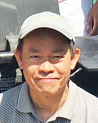 Dr. Luu Nguyen is the Director of Packaging, Quality, and Reliability at PsiQuantum since 2019, a start-up based in Palo Alto, CA, that aims at building the first large-scale, error-corrected, general-purpose silicon photonics-based quantum computer. He is a member of the IEEE Future Directions (FD) Committee. He’s also a co-lead of IEEE Quantum, an IEEE FD initiative launched to serve as IEEE’s leading community for all projects and activities on quantum technologies. He serves on the Steering Committee for IEEE Quantum Week, the flagship conference on all quantum computing and engineering topics, and participates in many IEEE technical committees (ECTC Packaging Technologies, TC on Reliability, TC on Emerging Technologies, Rel. for Electronics & Photonics Packaging Symposium), award committees (CPMT Field Award, SMTA Society Awards, and ASME Allan Kraus Thermal Management Award, EPPD Awards), and EPS Fellows Nomination committee. He’s currently an Associate Editor for T-CPMT and has been a Guest Editor for three past issues. Dr. Luu Nguyen is the Director of Packaging, Quality, and Reliability at PsiQuantum since 2019, a start-up based in Palo Alto, CA, that aims at building the first large-scale, error-corrected, general-purpose silicon photonics-based quantum computer. He is a member of the IEEE Future Directions (FD) Committee. He’s also a co-lead of IEEE Quantum, an IEEE FD initiative launched to serve as IEEE’s leading community for all projects and activities on quantum technologies. He serves on the Steering Committee for IEEE Quantum Week, the flagship conference on all quantum computing and engineering topics, and participates in many IEEE technical committees (ECTC Packaging Technologies, TC on Reliability, TC on Emerging Technologies, Rel. for Electronics & Photonics Packaging Symposium), award committees (CPMT Field Award, SMTA Society Awards, and ASME Allan Kraus Thermal Management Award, EPPD Awards), and EPS Fellows Nomination committee. He’s currently an Associate Editor for T-CPMT and has been a Guest Editor for three past issues.He retired as a Fellow at Texas Instruments in 2019, where he worked on various strategic initiatives that included sensors, printed electronics, high voltage packaging, wafer-level packaging, thermal management, design-for-manufacturability, and design-for-reliability. He has a Ph.D. in Mechanical Engineering from MIT and worked at IBM Research, Philips Research, and National Semiconductor. He co-edited two books on packaging technologies, has several book chapters, over 70 patents and invention disclosures, and over 200 publications. He is a Fellow of IEEE and ASME, a Fulbright Scholar (Finland 2002), a Fannie and John Hertz Fellow, and an AAAS Mass Media Science and Engineering Fellow. He received two Best Paper of Conference Awards, one Best Poster of Conference Award, and eight IMAPS and IEMT Best Session of Conference Awards. He received the 2004 IEEE CPMT Outstanding Sustained Technical Contributions Award, the 2015 IEEE Outstanding Engineering Manager Award for the IEEE Region 6, and the 2018 Surface Mount Technology Association Member of Technical Distinction. Other awards also include the 2003, 2014, 2015, and 2016 Mahboob Khan Outstanding Mentor Award from the Semiconductor Research Corporation to recognize contributions to student mentoring, research collaboration, and technology transfer. |
|
 Dr. Bindu R. Nair was appointed to the Senior Executive Service in March 2020 and is now serving as the Director of Basic Research within the Office of the Under Secretary of Defense. In this role, she is responsible for oversight and coordination of the Department’s $2.5 billion investment in basic science. This investment supports high risk and high pay-off basic research projects in fields including physical science, life science, environmental science, applied mathematics, and others that probe the limits of today’s technologies and discover new phenomena and know‐how that may ultimately lead to future technologies for the Department. Dr. Bindu R. Nair was appointed to the Senior Executive Service in March 2020 and is now serving as the Director of Basic Research within the Office of the Under Secretary of Defense. In this role, she is responsible for oversight and coordination of the Department’s $2.5 billion investment in basic science. This investment supports high risk and high pay-off basic research projects in fields including physical science, life science, environmental science, applied mathematics, and others that probe the limits of today’s technologies and discover new phenomena and know‐how that may ultimately lead to future technologies for the Department.From 2012-2017, Dr. Nair served in various roles including Acting Director and Deputy Director in the Human Performance, Training and Biosystems Directorate within the Office of the Secretary of Defense. In this role, Dr. Nair was involved in overseeing a broad range of DoD’s science and technology programs that support Warfighter effectiveness. Her specific areas of responsibilities in the office were in environmental technologies, bio-assist technologies (for exoskeletons and prosthetics), human machine teaming, and social behavioral modeling in the information environment. Prior to that assignment, Dr. Nair worked for the Department of the Army with oversight responsibilities over the science and technology program in power and energy. She has worked in the DoD laboratory system at Natick Soldier Research, Development and Engineering Center as well as in private industry at Foster Miller (Waltham, MA). Her research expertise is in the field of Materials Science and Engineering including nanomaterials, polymers, and organic electronic materials, and she has taught graduate level courses in Polymer Synthesis. She has published primarily in membrane and materials development fields and holds patents in fuel cell technologies. Dr. Nair holds a B.Sc. from the University of Florida and a Ph.D. from the Massachusetts Institute of Technology in Materials Science and Engineering. |
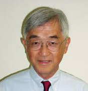 William Chen (Bill) holds the position of ASE Fellow & Senior Technical Advisor at ASE Group. Prior to joining ASE, he was Director at the Institute of Materials Research & Engineering (IMRE) in Singapore, following a distinguished career at IBM Corporation. Bill is a past President of the IEEE Electronics Packaging Society. He is a Life Fellow of IEEE and a Fellow of ASME. He received the ASME InterPACK Achievement Award in 2007. In 2018, he received the IEEE Electronics Packaging Field Award, recognizing his contribution to electronic packaging, from research & development through industrialization. William Chen (Bill) holds the position of ASE Fellow & Senior Technical Advisor at ASE Group. Prior to joining ASE, he was Director at the Institute of Materials Research & Engineering (IMRE) in Singapore, following a distinguished career at IBM Corporation. Bill is a past President of the IEEE Electronics Packaging Society. He is a Life Fellow of IEEE and a Fellow of ASME. He received the ASME InterPACK Achievement Award in 2007. In 2018, he received the IEEE Electronics Packaging Field Award, recognizing his contribution to electronic packaging, from research & development through industrialization.Bill chairs the Heterogeneous Integration Roadmap initiative, co-sponsored by 3 IEEE Societies (EPS, EDS & Photonics) together with SEMI & ASME Electronics & Photonics Packaging Division. |

 Kris Erickson is a Research Manager at Meta’s Reality Labs – Research, leading projects to develop materials & manufacturing solutions for next-generation XR hardware. He was previously at HP Labs leading materials and HW R&D teams developing metal 3D print, polymer 3D print and 3D printed electronics solutions. He obtained his PhD in Chemistry at the University of California, Berkeley researching nanomaterials and was a post-doctoral appointee at Sandia National Labs within the Materials Physics group.