Speaker: Harry Gee, ON Semiconductor

Presentation Slides: “Wafer-Level Process Formation of a Polymer-Isolated Chip-Scale Package” (1 MB PDF)
Meeting Date: Tuesday, November 22, 2016
Time: 11:30 AM Registration (and sandwiches/drinks); 12:00 PM Presentation
Presentation-only: 12:00 noon (come at 11:45)
Cost: $5 IEEE members. students, unemployed; $10 non-members

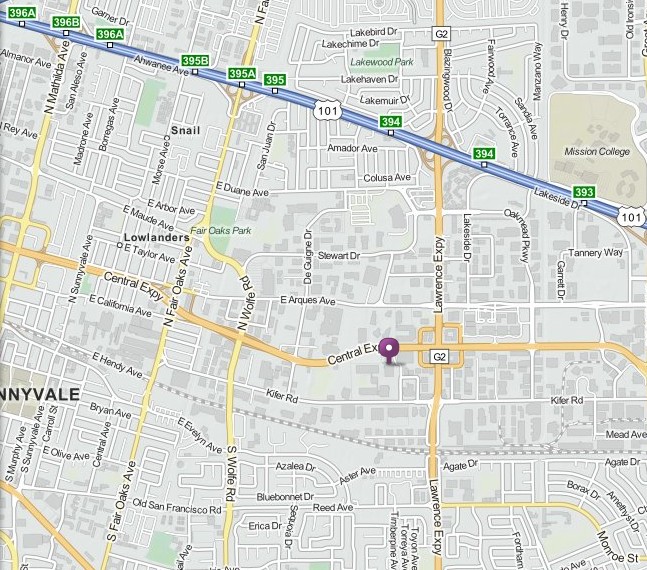
Location: Texas Instruments Building E Conference Center, 2900 Semiconductor Dr. (off Kifer Rd), Santa Clara
Reservations: 1611cpmt.eventbrite.com
Summary: Small-footprint (0201/01005 size) bare silicon chip-scale package (CSP) after board assembly has yield loss due to high leakage between an I/O pad and the silicon substrate. The solder paste applied at assembly can inadvertently extend out and touch the exposed silicon along the sidewall of the CSP device. After reflow, this excess solder may cause a high leakage path or short between an I/O pad and the silicon of the CSP device. Small-footprint CSP devices normally have I/O pads that are short and close to the CSP die edge. The short bump height and the proximity to the die edge increase the chance for a solder short to the silicon substrate along the sidewall. In this talk, we present a wafer-level backend process flow to make a 0201/01005 CSP device such that the silicon sidewalls and backside are completely covered by a thin non-conducting polymer material. The polymer-isolated CSP solution provides complete electrical insulation to the active silicon. This eliminates solder-to-silicon sidewall leakage yield loss after board assembly. The polymer offers protection to the active silicon device from assembly handling to prevent die cracking and chip-out. We will present assembly electrical yield and board level reliability results for this polymer-isolated CSP device made by wafer level processing.
Bio: Harry Gee is presently a Device Engineer at ON Semiconductor. He received his B.S. degree in Chemical Engineering from the University of California, Berkeley. He has been active in the semiconductor industry for over thirty years as Process, Device, and Development engineer. He has worked with Wafer-Level Chip-Scale Packaging (WLCSP) for the past sixteen years on numerous products from discrete parts to large analog/logic chips.
