— trade-offs, form-factor, functionality, flexible designs, real estate …
Speaker: Jim Moss, Texas Instruments

Sponsors: CPMT SCV Chapter, co-sponsored by PELS Chapter
Meeting Date: Thursday, July 28, 2016
Time: 11:30 AM Registration (and sandwiches/drinks); 12:00 PM Presentation
Presentation-only: 12:00 noon (come at 11:45)
Cost: $5 IEEE members. students, unemployed, $10 non-members
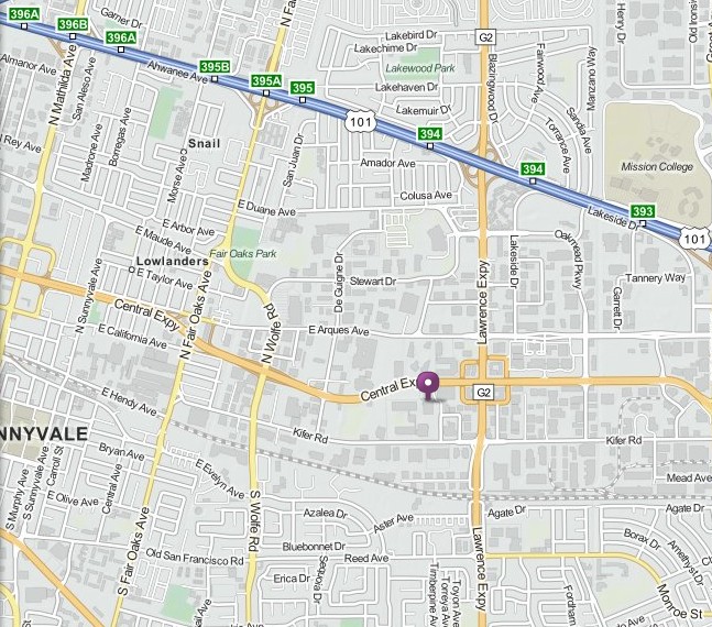
Location: Texas Instruments Building E Conference Center, 2900 Semiconductor Dr. (off Kifer Rd), Santa Clara
Reservations: 1607lcpmt.eventbrite.com
Summary: This talk will discuss volumetric co-design methodology and packaging construction trade-offs for 3D SiP power modules. It will provide more details on the SiP eco-system, co-design, construction, materials and circuit topology.
Today, designers are demanding an overall form-factor reduction to save board space, increase functionality, and allocate more real estate toward end-user applications — all with less space allocated to power management where not just the X-Y shrink but the 3D volumetric shrink is required also. For example, in wearable products, the semiconductor industry has recently seen an increase in the use of system-in-package (SiP) technology for users who want simpler, more flexible designs and need to fulfill challenging space requirements. And, we expect to see this trend continue.
Bio: Jim Moss is the Power Products Technology Manager in TI’s Silicon Valley Analog. He is currently working on high-power modules utilizing controllers, MOS & GaN FETs, and passives. He has over 35 years of experience in the semiconductor industry and with TI/National for more than 25 years.
His experience covers Power, Wireless/RF, x86, and microcontrollers. He has been working in Systems Design, Product, Test and various technical management roles. He holds an MS-EM from Santa Clara University and BS-EE from Illinois Institute of Technology.